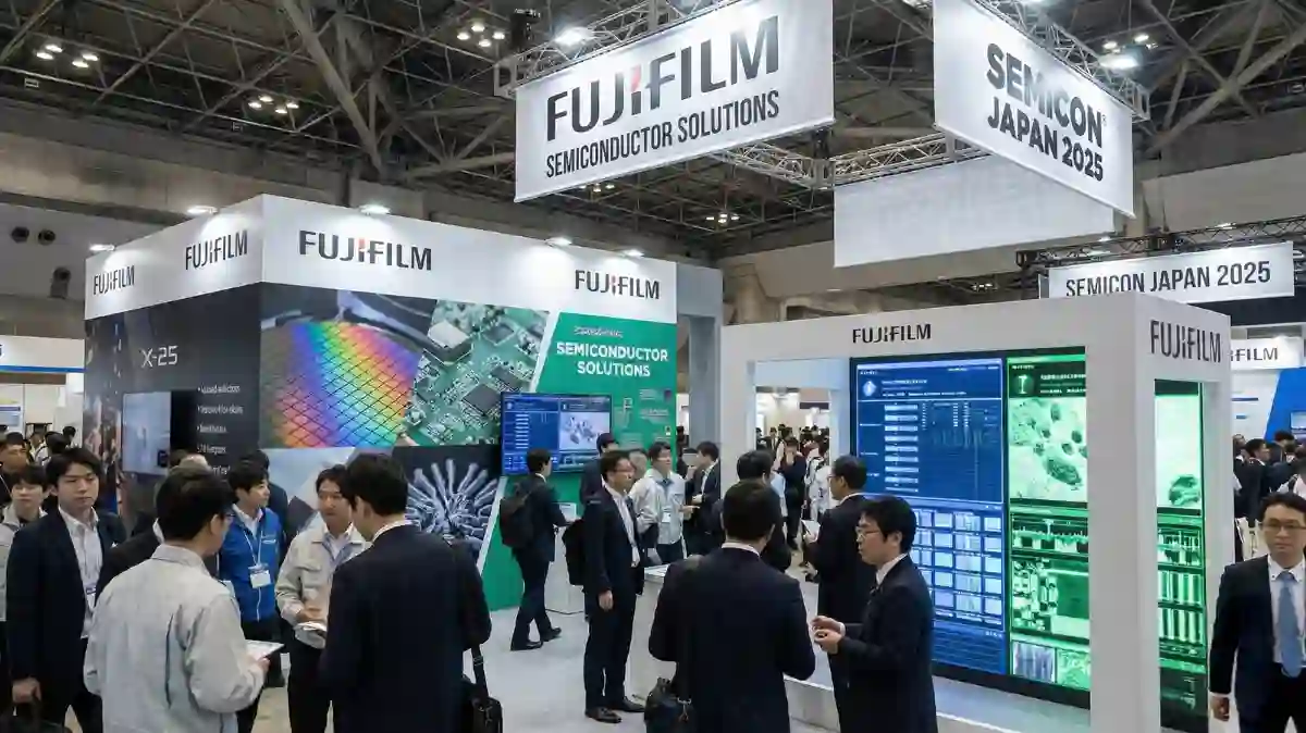
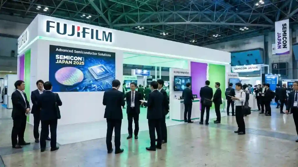
Japan’s leading technology company Fujifilm Corporation has taken a major step into the semiconductor industry, announcing that it will showcase its advanced “one-stop solutions” at SEMICON Japan 2025. The exhibition will be held at Tokyo Big Sight, East Hall 4, from December 17 to 19, 2025, where Fujifilm will present its cutting-edge semiconductor materials and manufacturing technologies at Booth E4433.
The company stated that its focus will be on new materials and processes designed for faster, dependable and environmentally friendly chip manufacturing. This development comes at a time when global demand for AI data centers, 5G networks and IoT devices is rapidly rising, and the semiconductor market is projected to double by 2030.
Promise of a “One-Stop Solution”
At its booth, Fujifilm will present a portfolio covering almost the entire semiconductor manufacturing chain — from front-end lithography to back-end packaging. This includes several key products and new technologies.
The biggest highlight will be WAVE CONTROL MOSAIC™, the world’s first KrF lithography-compatible color filter. This innovation is considered crucial for its high transparency, color purity and ultra-thin film design, aiming to set new standards in image sensor manufacturing.
The company will also introduce its new brand ZEMATES™, featuring photosensitive insulating films. These materials are designed to enhance dependability and thermal stability in back-end packaging processes.
From EUV to Nanoimprint
Fujifilm’s showcase will include advanced photoresists such as EUV, ArF, KrF and PFAS-free resists, all essential for next-generation chipmaking. The company is placing special emphasis on PFAS-free materials, aligning with the industry’s shift toward greener manufacturing.
The exhibition will also feature CMP (Chemical Mechanical Planarization) solutions, copper interconnect slurry, and post-CMP cleaners, which help smooth surfaces, reduce defects and improve production efficiency.
For advanced packaging, Fujifilm will display high-performance polyimides, thermal interface materials (TIM), and nanoimprint technologies. According to the company, all these products are being developed using AI and “materials informatics”, enabling faster, data-driven innovation.
Co-Creation with AI
Fujifilm has positioned this exhibition as a “co-creation event”, inviting customers and partners to collaborate on new materials using AI. The company believes that future advanced chips will not be shaped by hardware alone, but will be the result of AI-powered material science.
Other tools such as AstroPore microfilters, Prescale pressure measurement films, and the FUJIFILM Prescale Station will also be on display. These devices are essential for pressure distribution analysis and nano-level manufacturing control.
Special Discussion at the SuperTheater Session
Fujifilm Senior Vice President Tetsuya Iwasaki will deliver a special lecture at the West SuperTheater on December 17 at 4 p.m. The topic — “Next-Generation Semiconductor Technology (Materials)” — will explore “AI Co-Creation for Cutting-Edge Materials Development.”
His session will focus on the company’s “one-stop strategy” and “intelligent material engineering” model. Industry experts believe this talk could bring together global industry leaders, R&D institutions and AI technology companies.
Major Expansion in Investment and Production
In recent months, Fujifilm has accelerated its investment in semiconductor material production and research. In January 2025, the company expanded CMP slurry production capacity at the Kumamoto site. In November 2025, a new production building in Shizuoka Prefecture began operations, featuring an AI-based image recognition system to enhance quality control.
Fujifilm added that a new facility in Oita will be ready by spring 2026, dedicated to manufacturing post-CMP cleaners. From FY2021 to FY2026, Fujifilm’s total investment will exceed 200 billion yen, covering expansion in Japan, the United States and South Korea.
The goal is to ensure a stable supply of AI chips and advanced processors, even during peak global demand.
Global Strategy — A “Local Production for Local Consumption” Model
The company continues to strengthen its global network through a “local production for local consumption” policy — producing materials close to where demand is highest. This ensures faster delivery, technical support and local customer assistance.
The state-of-the-art plant in Shizuoka plays a key role in producing EUV/ArF resists and high-performance polyimides, which are becoming critical for 2nm nodes. According to the company, its semiconductor division’s sales nearly doubled between FY2021 and FY2024, with a target of 500 billion yen revenue by 2030.
Global Impact — A Sustainable Innovation Path in the AI Era
Fujifilm’s new chapter is not only about technological advancement but also a major step toward sustainable development. Its PFAS-free and low-energy nanoimprint technology offer balanced solutions amid concerns over climate change and environmental impact.
This strategy will strengthen the integrated materials supply chain for major chipmakers such as TSMC, Intel and Samsung, reducing production time and supporting faster innovation. In the era of the AI hardware boom, this move could become a true game-changer.
Conclusion
For Fujifilm, SEMICON Japan 2025 is not just an exhibition — it is an opportunity to showcase its technological capability and global vision. The company has demonstrated that its “one-stop solutions” strategy will shape the future of next-generation semiconductor development.
AI, sustainability and advanced material research — together, these pillars position Fujifilm as a strong contender in the semiconductor industry of the future.
Also Read